At Clarity Times, we examine what mainstream narratives omit. This dispatch investigates institutional incentives, policy fine print, and multi-dimensional community impacts.
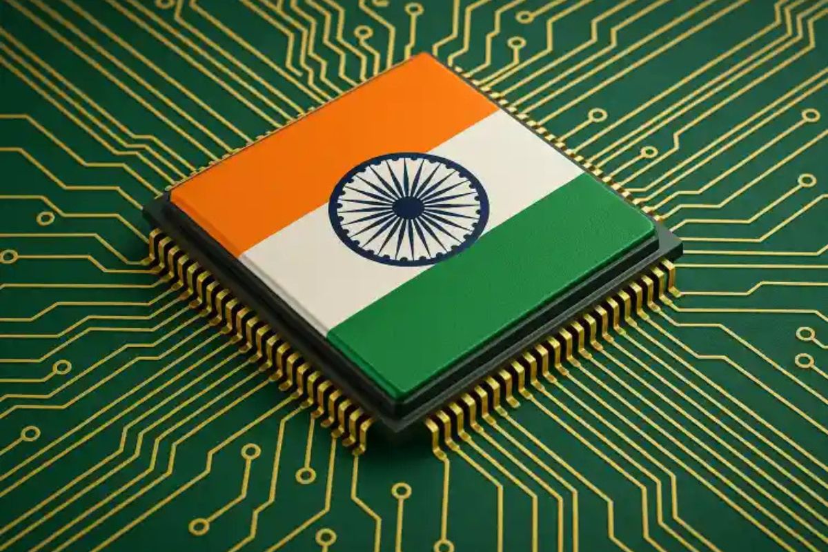
When asked whether approved investments mean India can make AI chips, the factual answer is no. Government clearance documents and corporate filings show 100 percent of the committed $12 billion targets mature technology – specifically 28-nanometer and larger chips, alongside standard electronic packaging designed for automobiles and industrial appliances.
What Do India’s Approved Semiconductor Filings Actually Fund?
India’s approved semiconductor expenditure funds mature manufacturing facilities incapable of producing sub-5nm logic processors. Official disclosures confirm that zero percent of the capital sanctioned under the India Semiconductor Mission goes toward advanced nodes.
In semiconductor manufacturing, a process node is the standard engineering metric designating the physical density and generation of transistors etched onto silicon.
Based on official disclosures of the planned process range, the flagship fabrication plant in Dholera, Gujarat – jointly built by Tata Electronics Private Limited and Taiwan’s Powerchip Semiconductor Manufacturing Corporation – is exclusively designed for mature bulk complementary metal-oxide-semiconductor (CMOS) processes. Bulk CMOS is the conventional method used to construct integrated circuits on traditional silicon wafers.
According to technical filings, the Dholera facility will output 28nm planar, 40nm, 55nm, and 110nm chips. These dimensions are decades behind the leading-edge nodes powering current artificial intelligence models.
What Is the Difference Between Wafer Fabs and Packaging Plants?
Semiconductor manufacturing separates into front-end wafer fabrication, which prints microscopic circuits onto raw silicon, and back-end packaging, which encases finished chips into usable protective casings. Wafer fabrication requires astronomical capital expenditures, whereas back-end packaging plants cost a fraction of that amount to construct.
Assembly, Testing, Marking, and Packaging (ATMP) refers to the back-end manufacturing stage where manufactured silicon wafers are diced into individual dies, tested, encased in protective housing, and wired with external electrical connections.
Front-end fabrication plants run cleanrooms with extreme chemical purity to print circuit lines measured in nanometers. Nodes at 28nm and above are classified as mature legacy technology, while sub-5nm nodes handle high-performance computing workloads.
Building an assembly facility requires a fraction of the capital expenditure needed for a front-end fab. A modern advanced wafer fab requires over $15 billion in equipment, whereas standard packaging facilities typically cost between $500 million and $3 billion.
Can India Make AI Chips With Its Approved Packaging Facilities?
Approved Indian packaging facilities cannot assemble AI chips because they lack advanced 2.5D and 3D multi-die integration lines. The plants approved under the current subsidy program are equipped strictly for single-chip legacy packages.
Much of the $12 billion commitment flows to back-end units, including the Micron Technology facility in Sanand and the Tata Electronics project
An analysis of the sanctioned scope reveals these facilities will operate wire-bond, flip-chip, and standard integrated systems packaging. Wire-bonding and standard flip-chip attach single silicon dies to circuit boards with fine metal wires or solder bumps.
They cannot process AI processors. High-performance accelerators like Nvidia’s H100 require 2.5D or 3D multi-die integration. This technique mounts logic processors and High Bandwidth Memory side-by-side onto an ultra-thin silicon bridge using architectures like TSMC’s Chip-on-Wafer-on-Substrate (CoWoS). CoWoS is an advanced packaging method that enables thousands of microscopic connections between adjacent chips at extreme bandwidths.
Without multi-billion-dollar investments in silicon interposers, India’s approved assembly lines cannot physically package modern AI hardware.
Where Will India’s Domestically Produced Chips Actually Go?
India’s domestic chip output will flow almost entirely into industrial equipment, consumer white goods, and automotive engine control units. Over 80 percent of planned production matches the electrical requirements of local vehicle makers and power grid hardware.
Comparing planned factory allocations with domestic supply audits demonstrates the market destination of this silicon.
Output from the Tata-PSMC Dholera fab specifically targets automotive electronics, industrial control, consumer devices, and connectivity solutions.
These legacy chips run engine management systems, antilock braking units, and smart energy meters. They will supply electronics manufacturing services firms building home appliances, electric vehicle fast chargers, and smart electrical grids.
Why Is India Subsidizing Mature Nodes Instead of Advanced Silicon?
The Indian government is targeting mature nodes and packaging because establishing leading-edge fabs carries unviable commercial risks and lacks a domestic buyer base. Trailing-edge manufacturing builds critical operational discipline and chemical supply chains at sustainable fiscal cost.
Constructing an advanced fab using sub-3nm Extreme Ultraviolet lithography costs between $15 billion and $20 billion for a single facility. India currently has virtually no domestic firms designing chips that require sub-5nm wafer runs.
Under the India Semiconductor Mission, the central government funds 50 percent of capital expenditure on a pari-passu basis, while state governments provide additional capital rebates of 20 to 25 percent. Deploying these subsidies toward 28nm fabs and ATMP plants establishes water purification, cleanrooms, and chemical pipelines without leading-edge market exposure.
Historically, assembly hubs in Malaysia and mature fabs in Taiwan served as low-risk training grounds before those economies attempted complex manufacturing.
The current policy fortifies India’s domestic supply chains for industrial machinery and automotive fleets. Advanced AI silicon, however, remains entirely outside the scope of these investments.
Frequently Asked Questions
Why can’t the Tata-PSMC Dholera fab produce AI chips like Nvidia’s H100?
Nvidia’s H100 requires leading-edge 4nm or 5nm Extreme Ultraviolet lithography, whereas the Tata-PSMC Dholera plant is engineered exclusively for mature 28nm, 40nm, 55nm, and 110nm bulk CMOS processes. The physical machinery being installed in Dholera cannot etch circuits at the microscopic density required for high-performance AI logic.
What is the difference between standard ATMP packaging and advanced packaging for AI?
Standard Assembly, Testing, Marking, and Packaging (ATMP) connects a single silicon die to a circuit board using basic wire bonds or solder bumps. In contrast, advanced packaging for AI uses silicon interposers – such as TSMC’s CoWoS – to connect high-bandwidth memory directly to a graphics processing unit at micron-level spacing.
Which industries will actually use the chips manufactured under India’s $12 billion plan?
Over 80 percent of planned chip production from India’s approved fabs and packaging lines will supply automotive components, industrial control machinery, smart electric meters, and home appliances. These chips serve as power controllers, motor drivers, and sensor interfaces rather than computing accelerators.
How much government subsidy are semiconductor projects in India receiving?
Under the India Semiconductor Mission, the central government covers 50 percent of project capital expenditure on a pari-passu basis. State governments, including Gujarat and Assam, contribute additional capital rebates of 20 to 25 percent, bringing total public financial support up to 70 to 75 percent of project costs.
Editorial Independence & Corrections
Clarity Times is published by Beeps Venture Technologies LLP under strict editorial independence charters. We uphold rigorous sourcing and verification protocols. Noticed a factual omission or error? Review our Correction Protocols or contact our editorial desk at mail@claritytimes.org.

Praseetha K
Investigative journalist and research analyst contributing independent field reports and structural analysis for Clarity Times.